The American Institute for Manufacturing Integrated Photonics (AIM Photonics) and Analog Photonics (AP) today announced the release of the AP SUNY Process Design Kit v2.5a (APSUNY_PDKv2.5a). This latest release expands the comprehensive set of Silicon Photonics Integrated Circuit (PIC) component libraries within SUNY Poly’s process capabilities to address the needs for O+C+L band applications. Combined with Multi-Project Wafer (MPW) runs, this updated PDK will give AIM Photonics’ members access to world-class silicon photonics components for the development of optical transceivers or systems used in all levels within data centers and high-performance computers.
AIM Photonics Design and Multi Project Wafers
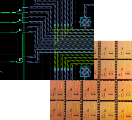
The Silicon Photonics PDK includes design guide, design rule check deck, technology files, active and passive component documentation, abstracts, schematics, and compact models for the development of PICs.
The key features of the APSUNY_PDKv2.5a are:
- O Band modulation, detection and coupling support.
- C+L Band modulation, detection, filtering, switching, monitoring and coupling support.
- Single-level and Multi-level modulation format support at 50Gbps, namely NRZ and PAM-4.
- Continued multi-vendor Electronics-Photonics-Design-Automation (EPDA) support with integrated EPDA PDK flow for hierarchical design and system-level simulation.
Read more...